Projects
-
- 2025 - 2027
- RFIC
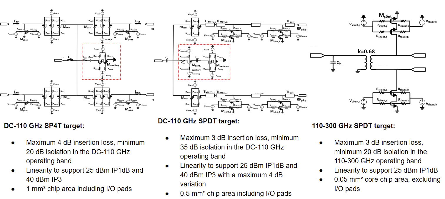
Developement of DC-300 Ghz SPDT and SP4T switches using SOI CMOS technology
While developing next-generation RF switch modules, the main focus is to cover a wide frequency range, meeting the specific needs of various industrial applications. The RF switch modules to be designed in this context are projected to be used in multiple industrial applications, and the RF switch structures will be integrated in a manner compatible with SOI (Silicon on Insulator) technologies. The main challenge in designing RF switches is achieving high linearity, low input loss, and excellent isolation while working effectively at both high frequencies like millimeter waves and relatively low frequency ranges like 1 GHz .These switches will not only feature wideband characteristics but also, thanks to unique circuit performance adjustability, will provide optimized performance parameters in target frequencies for various industrial applications such as satellite communications between 3 GHz and 30 GHz, mobile communications between 600 MHz and 6 GHz, medical imaging between 1 GHz and 10 GHz, automotive radars between 70 GHz and 110 GHz, airport security systems, quantum qubit control systems, and distributed communication systems above 110 GHz. Moreover, the targeted RF switch circuits will be measured using flip-chip or bond wire depending on the frequency they will operate at.
Ongoing -
- 2024 - 2027
- RFIC
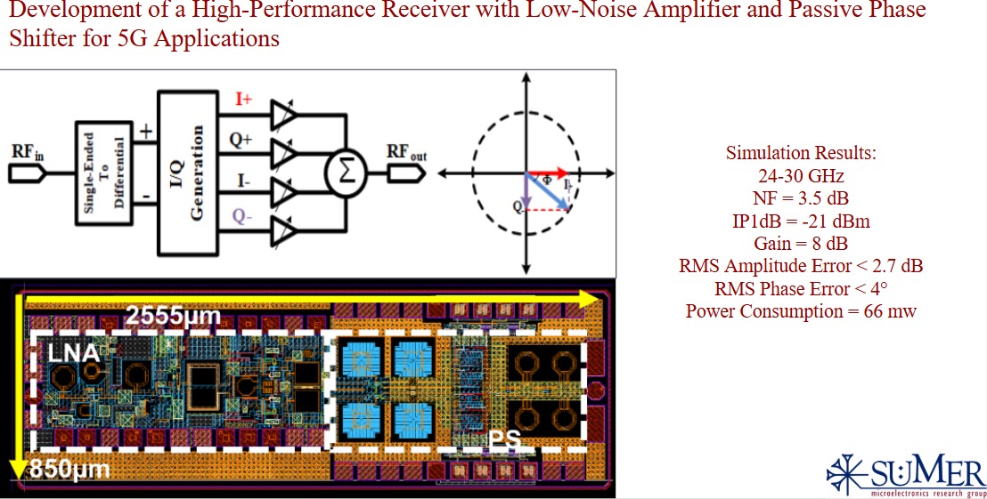
Development of a High-Performance Receiver with Low-Noise Amplifier and Passive Phase Shifter for 5G Applications
The objective of the project is to design a high-performance receiver module for 5G communication systems, integrating a low-noise amplifier (LNA) with a passive vector-sum phase shifter (VSPS). The receiver utilizes a three-stage architecture, where the signal is split and processed across multiple stages to achieve the desired phase and amplitude modifications. This design aims to minimize phase and amplitude errors, ensuring high resolution for optimal system performance. The receiver module is optimized for operation in the 24-30 GHz frequency range, with a focus on low noise figure (NF), high gain, and linearity. The LNA plays a critical role in reducing the overall noise of the system while compensating for any losses due to the phase shifting process generated by the VSPS.
Ongoing -
- 2022 - 2025
- Neural Networks
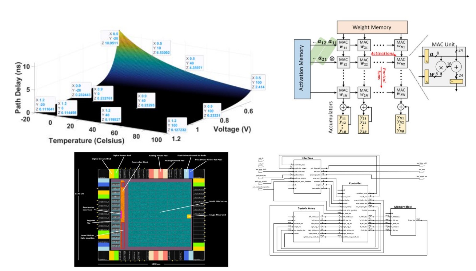
Development of process, voltage and temperature variationaware highly energy-efficient deep neural networks with high inference accuracy for internet-of-things applications
The project aims to develop probabilistic timing error models and FPGA-based deep learning accelerators for energy-efficient AI applications. Significant progress has been made, with 95% completion of a probabilistic error model that outperforms traditional Monte Carlo simulations in speed and efficiency, enabling faster and more accurate error prediction. The 16x16 MAC array accelerator prototype has been successfully designed and fabricated, with testing and PCB integration in progress. Deep learning models, including MobileNet, ResNet, and Inception, have been optimized for FPGA-based inference on AMD Xilinx Kria K26 SOM, achieving up to 8x speed improvement over initial implementations, though further optimizations are needed to surpass CPU performance. Additionally, the project's breakthroughs in error modeling and AI acceleration have the potential to enhance IoT and high-performance computing applications.
Ongoing -
- 2021 - 2023
- Sensor
Development of Plasmon-enhanced HOT MIR Photodetectors
The aim of the project is to develop plasmon-enhanced HOT MIR (High Operation Temperature Mid-Infrared, 3–16 μm) photodetector. The performance of the conventional HOT MIR photodetectors is limited by a large thermal generation and recombination rate of charge carriers in narrow gap semiconductors used as absorbers of the devices which reduces the responsivity of the devices and makes them very noisy. This can be prevented by using optimized A3B5 materials and reduction of the absorber volume (thickness and area) where thermal generation occurs, while keeping quantum efficiency and apparent optical detector area unchanged. The absorber thickness can be reduced by using a plasmonic subwavelength hole array. Subwavelength hole array design will be used to confine the incoming light in a thin absorber due to the surface plasmon polaritons. The small thickness of the absorber solves also the poor collection of photogenerated charge carriers’ issue. The solutions will lead to HOT MIR photodetectors with performance close to theoretical limits. In that way, it will be possible to improve the responsivity, the signal-to-noise ratio and response time at ambient temperature or temperatures achievable with Peltier coolers (190 to 325 K).
Completed -
- 2019 - 2022
- ROIC
2-GSPS 8-bit Asynchronous Time-Interleaved Successive Approximation Register (SAR) Analog-to-Digital Converter (ADC) for MM-wave Radar and Wideband Communication Applications
The aim of the project is to develop a high-speed (2-MSPS) 8-bit asynchronous time-interleaved successive approximation register (SAR) analog-to-digital-converter (ADC) for mm-wave radar and wideband communication systems such as WiGig and 5G. The proposed ADC will have 8 sub-ADC channels for time-interleaving to operate at 2 GSPS high sampling rate, will also use offset, linearity and clock skew calibration techniques to improve the overall performance of the ADC. The proposed SAR ADC will consume low power (20mW), will have high energy efficiency (77 fJ/conv-step) and will occupy small chip area (0.5 mm2) due to newly developed full custom SAR control unit and will be fabricated in 65 nm CMOS process technology.
Completed -
- 2019 - 2023
- RFIC
Wideband Low Noise X-to-K Band SiGe BiCMOS T/R Module Core-Chip
Next generation phased arrays require new specifications with the improvements in the technology, that are enabling multi-functionality and multi-band operation to be capable of multi-beam formation at various frequencies for applications. Wideband operation is one of the main requirements of the new generation systems in single-beam operations and electronic warfare applications to form multi-purpose systems; single band designs can be replaced with a single multi-band chip, which presents cheaper solutions for space-satellite applications, 5G and beyond communication and military based radars. The project proposes a X-to-K band T/R module core-chip to satisfy the system requirements as following; Compact size multi band low power dissipation, low receiver NF, high phase (delay)/ amplitude resolution and high transmitter output power. Although III-V technologies satisfy the RF specifications, they are contradicting with the compactness and low-cost expectations which prevents them from broadening its market to commercial applications. In this project, a novel SiGe BiCMOS T/R core-chip is proposed, which targets system and circuit level solutions on the described content. The corechip is going to include basic sub-blocks in a half-duplex array with All-RF architecture.
Completed -
- 2020 - 2023
- RFIC
Low-Noise High Linearity Amplifiers for 5G MassMIMO and Low-Noise mm-wave 5G Amplifiers
5G applications have pushed for higher data rate requirements with each new generation. The demand for increased data rates has not only increased expectations of the noise performance of LNA but also created a demand for increased communication distances which have attracted attention to massive multiple-input-multiple-output (MIMO) systems. MIMO systems have introduced a new challenge for modern receiver chains, an increased linearity requirement since a stronger interferer resistance is required with each new channel in the 5G frequency regions. In this project, the design of high-linearity low-noise amplifiers is aimed. The project focuses on the design of an LNA for the Sub-6 GHz bands of the 5G communication systems and another LNA for the 5G bands in the frequency range of 24-30 GHz.
Completed-
Funding Agency:
Analog Devices Inc.
-
-
- 2018 - 2020
- RFIC
4 Channel MIMO System for 5G Communication
The main goal of this project is the design of four channel element of MIMO array ,which will be utilized in the next generation communication systems, and up/down converter mixers to be used in these systems. The four channel MIMO element and mixers are designed in IHP 0.13μm SiGe BiCMOS technology. Both transmitter and receiver chains include PS, attenuator and VGA for phase and amplitude control. As an amplifier, the receiver chain has LNA at the input of the channel while the transmitter chain has PA at the output. The objectives of this part of the project are the integration and verification of each channels and the formation of combined 4 channels of Tx and Rx.
Completed -
- 2018 - 2020
- RFIC
In-Band Full-Duplex for 5G Communication systems
In-Band Full-Duplex (IBFD) operations enable to overcome the challenges of 5G communication systems. To achieve IBFD operation, the leakage of transmitted signal to the receiver side should be suppressed. The main goal of this project is the design of IBFD transceiver used in 5G communication systems. This transceiver consists of tunable Electrical Balance Duplexer (EBD) which is the core of the suppression of the leakage, an LNA and a PA. The objectives are the verification of each sub-block in the system and then, the verification of an integrated system performance. The project utilizes IHP 0.13μm SiGe BiCMOS process technology. This work is carried out in collaboration with an Industry Partner.
Completed -
- 2015 - 2018
- RFIC MEMS
SiGe BiCMOS Technology Based Monolithic 140 GHz and 240 GHz (THz) Frontend Circuits
The main goal of this project is the use of 0.13 um SiGe BiCMOS process technology / devices to realize single-chip, high performance THz circuits and systems for different applications, including new solutions in radiometry for imaging and spectroscopy for characterization applications. In addition to standard technology devices, the use of integrated RF-MEM switches and tunable capacitors are part of the project aim to further enhance the monolithic system solution/performance. This work is carried out in collaboration with Dr. Volkan Ozguz (PI), Sabanci University Nanotechnology Center, and IHP Microelectronics (Germany).
Completed -
- 2016 - 2019
- Sensor ROIC
Development of High Performance SiGe Bolometer IR Detectors and Arrays for Imaging Module Applications
Our aim in this project is multifold: (a) model the concentration of Ge in the SiGe alloy to optimize/maximize the temperature coefficient of resistance (TCR) of SiGe alloy, (b) apply the TCR optimized SiGe alloy for the development of SiGe -Multiple Quantum Well (MQW) bolometers for the minimum NETD, (c) apply NETD optimized, SiGe -Multiple Quantum Well bolometers for the realization of IR detector arrays with the-state-of- the-art pitch size, and finally (d) Development of Readout Integrated Circuits (ROICs) to complement SiGe-IR Bolometer Detector Arrays for the realization of uncooled-high performance and / or low cost LWIR IR Imaging Modules. The project targets TCR of 4.5%-5% and with an NETD value of 50mK. The framework of project also includes hybridization and packaging the detector arrays and the readout circuits in a vacuumed environment, as part of the integrated imaging module prototype developments. This work is carried out in collaboration with Dr. Javed Hussain Niazi KM (PI), Sabanci University Nanotechnology Center, and IHP Microelectronics (Germany).
Completed -
- 2015 - 2018
- RFIC
Design of fully integrated 94 GHz radiometer for passive millimeter wave imaging using SiGe BiCMOS technology
The aim of this project is design of a low NETD (Noise Equivalent Temperature difference) mm-wave radiometer which is used in passive imaging systems. In this project, first of all, the sub blocks of a single chip 94 GHz direct detection radiometer system - such as on chip antenna, LNA, power detector, SPDT and baseband blocks are designed, optimized, fabricated, tested and verified. High performance HBT's of the-state-of-the-art IHP 0.13μm SiGe BiCMOS process is used. As second objective, all of the blocks are integrated to a single chip and verified. As third objective, 2x2 arrays will be formed by this radiometer.
Completed-
Funding Agency:
TÜBİTAK
-
- 2014 - 2017
- ROIC
Low Power Digital ROIC Architectures and Pixel Core Development for LWIR and MWIR Imaging Applications
This project aims to develop low power digital readout integrated circuit (DROIC) architectures for LWIR and MWIR bands to be used in cryogenic temperatures. For the LWIR band, a new pixel parallel conversion with coarse and fine quantization is proposed based on PFM architecture.With the proposed architecture it is aimed in this project to achieve 100fJ/LSB with 15-bit resolution. Pixel pitch is as small as 15µm in MWIR spectrum (and even smaller) and it is not feasible to put all of the PFM structure under this pixel area. Additionally, it is hard to design 15-bit ADCs with megapixel arrays to support 400Hz frame rate and low power dissipation. The proposed method is to do pixel level coarse quantization using PFM and lower resolution column based ADCs. Since the resolution of column based ADCs is reduced, they can operate at higher speeds with lower power dissipation. The project is implemented in standard CMOS technologies with 16x16 and 32x32 test arrays.
Completed-
Funding Agency:
TÜBİTAK (P.I. Prof. Volkan Ozguz)
-
- 2014 - 2017
- Biosensor
Development of Hand-Held Lab-on-a-chip for the Detection and Quantification of Cancer and Cardiovascular Risk Markers
Completed-
Funding Agency:
TÜBİTAK
-
-
- 2015 - 2016
- RFIC
Design and Development of X Band Phase Shifter and Attenuator in SiGe BiCMOS Technology
Completed-
Funding Agency:
-
- 2013 - 2015
- ROIC
Low Quantization Noise and High Charge Storage Capable Digital CMOS ROIC Development for 640x512 LWIR Detectors
Completed-
Funding Agency:
ASELSAN A.Ş. and Ministry of Industry - SANTEZ National Program
-
- 2013 - 2015
- ROIC
Low Power, TDI Based Digital ROIC for Scanning 720x8 LWIR Detectors
Completed-
Funding Agency:
ASELSAN A.Ş. and Ministry of Industry - SANTEZ National Program
-
- 2013 - 2015
- ROIC
High Dynamic Range (Dual Band) and High SNR ROIC
Completed-
Funding Agency:
ASELSAN A.Ş. and Ministry of Industry - SANTEZ National Program
-
- 2012 - 2014
- ROIC
Digital CMOS ROIC with Low Quantization Noise and Charge Storage Capability for IR Imaging Systems
Completed-
Funding Agency:
TÜBİTAK
-
- 2007 - 2010
- Biosensor
RF Transmitter Based Transducer for Biosensor Applications
Completed-
Funding Agency:
TÜBİTAK
-
- 2010 - 2013
- RFIC
X-Band Phase Array Transceiver Module Using SiGe BiCMOS and RFMEMS Technologies
A transmit/receive module for X-band (8-12 GHz) phased arrays was developed in a 0.25-um SiGe BiCMOS process. The module included a low-noise amplifier (18-22 dB gain, <2 dB NF), a power amplifier (20 dB gain, 20 dBm OP1dB), a 4-bit digitally-controlled passive phase shifter (3-11° RMS phase error, 10-20 dB insertion loss), a variable gain amplifier to compensate PS gain variations and SPDT switches (<2.3 dB insertion loss,>25 dB isolation) to route the signals between TX and RX. The overall T/R module occupies an area of 1.75 x 2.8 = 4.9 mm2. Pad-to-pad measurements demonstrated a gain of 10-11 dB, noise figure of 4-6 dB and IIP3 of -10 dBm in receive mode. In transmit mode, the module achieved a gain of 10-12 dB and OP1dB of 16 dBm. The total power consumption of the chip is 285 mW.
Completed-
Funding Agency:
TÜBİTAK
-
- 2005 - 2008
- Biosensor
Protein microchip design; cardiovascular risk assessment platform
Completed-
Funding Agency:
DPT
-
- 2005 - 2007
- Biosensor
BioSensor Development using optical transduction for the detection of cardiovascular risk markers
.
Completed-
Funding Agency:
TÜBİTAK
-
-
- 2006 - 2008
- ROIC
TDI-Based Readout Integrated Circuit Development for 288x4 IR Detectors
Completed-
Funding Agency:
-
-
- 2006 - 2009
- RFIC MEMS
Development of High Performance Transceiver Sub-Circuits and RF MEMS Passives for IEEE 802.11a/15
Completed-
Funding Agency:
TÜBİTAK
-
- 2001 - 2004
- ROIC
Development of micromachined chemical sensors and signal read-out circuitry
Completed-
Funding Agency:
TÜBİTAK


